ACS Nano Cover Page for "An Atomistic Model of Field-Induced Resistive Switching in Valence Change Memory"
The publication "An Atomistic Model of Field-Induced Resistive Switching in Valence Change Memory" authored by M. Kaniselvan, M. Luisier, and M. Mladenovic has been selected as cover article of the current issue of ACS Nano.
A team of researchers from the Integrated Systems Laboratory at ETH Zurich, led by Prof. Mathieu Luisier and supported by the Werner Siemens Foundation, has developed a fully-atomistic model to simulate valence change memory (VCM) cells, an emerging technology with promising applications in modern computer architectures. The quest for scalable and cheap memory cells that can be integrated into in-memory or neuromorphic computing frameworks has boosted the development of novel types of memory cells, including VCM cells. The operational mechanism of VCM cells is based on the re-arrangement of a conductive filament composed of oxygen vacancies, allowing for at least two distinctive conductive states, ON and OFF. Many details behind the underlying diffusion of ions/vacancies and their interplay with electrons remain unknown, hindering the progress towards the commercialization of VCM cells.
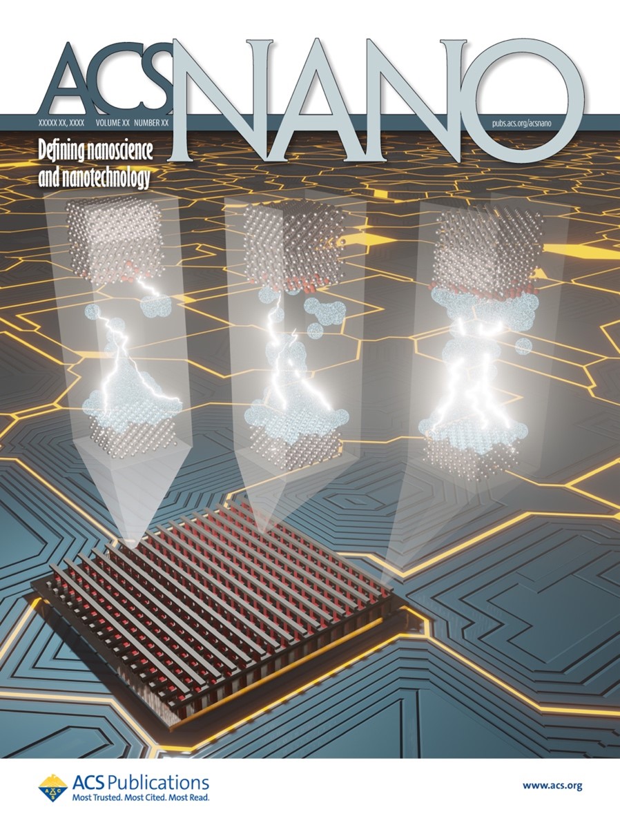
The ETH model proposed by Dr. Marko Mladenovic, a post-doc funded by the Werner Siemens Foundation, and Ms. Manasa Kaniselvan, a PhD student, can address these issues. It operates on real atomistic positions and combines different simulation methods, such as molecular dynamics, density functional theory, kinetic Monte Carlo code, and quantum transport. It is the first one to establish a direct link between the atomic changes in the structure of the material and the “current vs. voltage” characteristics of the resulting device. Furthermore, the team was able to precisely visualize the electrical current flow through the device, identifying the paths followed by electrons at the atomistic resolution. The model can be applied to different materials and device architectures, which is key to provide experimentalists with accurate design guidelines and devices with better performance.
The results obtained in this study were published in ASC Nano in 2023 (external pagehttps://doi.org/10.1021/acsnano.2c12575) and were selected as cover art for the May 9th 2023 issue of the magazine.